

The PCB design process consists of a series of industrial design steps and is a key link in ensuring the quality of high-volume circuit board products and reducing troubleshooting. PCBs are the foundation of industrial electronics design. Whether it is small batch production or mass production of consumer electronics, PCB design is involved in almost all design techniques. Due to the intricacies of the design process, many common mistakes recur. The five most common design problems and corresponding countermeasures in PCB design are listed below.
01 Pin error
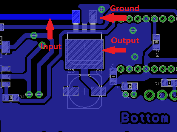
The series linear regulated power supply is cheaper than the switching power supply, but the power conversion efficiency is low. Typically, many engineers choose to use linear regulated power supplies because of their ease of use and low cost. But it should be noted that although it is very convenient to use, it consumes a lot of electricity and causes a lot of heat dissipation. In contrast, switching power supplies are complex in design, but more efficient. However, it should be noted that the output pins of some regulated power supplies may be incompatible with each other, so you need to confirm the relevant pin definitions in the chip manual before wiring.
02 Wiring error
Comparing differences between design and routing is a major error in the final stages of PCB design. So some things need to be double checked, such as device size, via quality, pad size, and review level. In short, repeated confirmation checks are required against the design schematic.
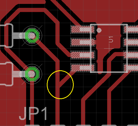
03 Corrosion Trap
When the angle between the PCB leads is too small (acute angle), corrosion traps (Acid Trap) may be formed. These sharp-angled connections may have residual etchant during the corrosion stage of the circuit board to remove more copper deposits there, thereby forming stuck points or traps. In the later stage, the lead wire may be broken, resulting in an open circuit. This corrosion trap phenomenon is greatly reduced due to the use of photosensitive etching solutions in modern manufacturing processes.
04 Tombstone device
When using the reflow process to solder some small surface mount devices, the device will form a single-ended lift phenomenon under the infiltration of solder, commonly known as "tombstone". This phenomenon is usually caused by an asymmetrical routing pattern, resulting in uneven heat spread across the device pads. Tombstones can be effectively mitigated with the correct DFM checks.
05 Lead Width
When the current of the PCB leads exceeds 500mA, the first wire diameter of the PCB will appear insufficient capacity. With typical thickness and width, the wires on the surface of the PCB can carry more current than the wires inside the multilayer circuit board, because the surface leads can dissipate heat by air flow. The width of the line is also related to the thickness of the copper foil on the layer. Most PCB manufacturers allow you to choose from 0.5 oz/sq.ft to 2.5 oz/sq.ft of different thicknesses of copper foil.